- 您现在的位置:买卖IC网 > Sheet目录3871 > PIC18F1230T-I/ML (Microchip Technology)IC PIC MCU FLASH 2KX16 28QFN
2009 Microchip Technology Inc.
DS39758D-page 19
PIC18F1230/1330
2.3
Master Clear (MCLR) Pin
The MCLR pin provides two specific device
functions: Device Reset, and Device Programming
and Debugging. If programming and debugging are
not required in the end application, a direct
connection to VDD may be all that is required. The
addition of other components, to help increase the
application’s resistance to spurious Resets from
voltage
sags,
may
be
beneficial.
A
typical
configuration is shown in Figure 2-1. Other circuit
designs may be implemented, depending on the
application’s requirements.
During programming and debugging, the resistance
and capacitance that can be added to the pin must be
considered. Device programmers and debuggers drive
the MCLR pin. Consequently, specific voltage levels
(VIH and VIL) and fast signal transitions must not be
adversely affected. Therefore, specific values of R1
and C1 will need to be adjusted based on the
application and PCB requirements. For example, it is
recommended that the capacitor, C1, be isolated from
the MCLR pin during programming and debugging
operations by using a jumper (Figure 2-2). The jumper
is replaced for normal run-time operations.
Any components associated with the MCLR pin
should be placed within 0.25 inch (6 mm) of the pin.
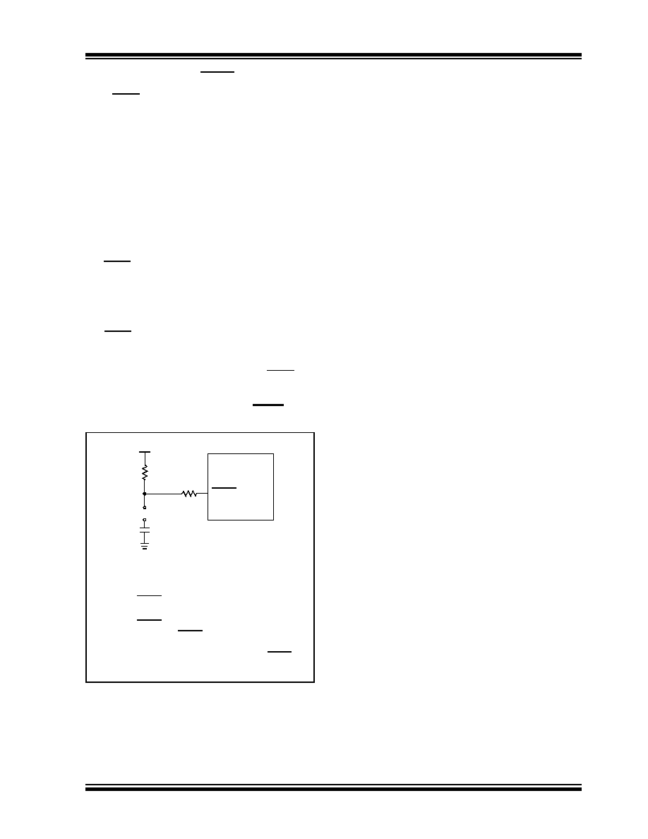
FIGURE 2-2:
EXAMPLE OF MCLR PIN
CONNECTIONS
2.4
ICSP Pins
The PGC and PGD pins are used for In-Circuit Serial
Programming (ICSP) and debugging purposes. It
is recommended to keep the trace length between the
ICSP connector and the ICSP pins on the device as
short as possible. If the ICSP connector is expected to
experience an ESD event, a series resistor is recom-
mended, with the value in the range of a few tens of
ohms, not to exceed 100.
Pull-up resistors, series diodes, and capacitors on the
PGC and PGD pins are not recommended as they will
interfere with the programmer/debugger communica-
tions to the device. If such discrete components are an
application requirement, they should be removed from
the circuit during programming and debugging. Alter-
natively, refer to the AC/DC characteristics and timing
requirements information in the respective device
Flash programming specification for information on
capacitive loading limits and pin input voltage high (VIH)
and input low (VIL) requirements.
For device emulation, ensure that the “Communication
Channel Select” (i.e., PGCx/PGDx pins) programmed
into the device matches the physical connections for
the ICSP to the Microchip debugger/emulator tool.
For
more
information
on
available
Microchip
development tools connection requirements, refer to
.
Note 1:
R1
10 k is recommended. A suggested
starting value is 10 k
. Ensure that the
MCLR pin VIH and VIL specifications are met.
2:
R2
470 will limit any current flowing into
MCLR from the external capacitor, C, in the
event of MCLR pin breakdown, due to
Electrostatic Discharge (ESD) or Electrical
Overstress (EOS). Ensure that the MCLR pin
VIH and VIL specifications are met.
C1
R2
R1
VDD
MCLR
PIC18FXXXX
JP
发布紧急采购,3分钟左右您将得到回复。
相关PDF资料
PIC18F1230T-I/SO
IC PIC MCU FLASH 2KX16 18SOIC
PIC18F1330T-I/ML
IC PIC MCU FLASH 4KX16 28QFN
PIC18F65J50T-I/PT
IC PIC MCU FLASH 16KX16 64TQFP
PIC18F83J11T-I/PT
IC PIC MCU FLASH 4KX16 80TQFP
PIC16LF627-04/P
IC MCU FLASH 1KX14 COMP 18DIP
PIC18F86J55T-I/PT
IC PIC MCU FLASH 48KX16 80TQFP
PIC18F43K22-I/MV
MCU PIC 8KB FLASH 40QFN
PIC16C55A-04I/P
IC MCU OTP 512X12 28DIP
相关代理商/技术参数
PIC18F1230T-I/SO
功能描述:8位微控制器 -MCU 4KB Flash 256 RAM RoHS:否 制造商:Silicon Labs 核心:8051 处理器系列:C8051F39x 数据总线宽度:8 bit 最大时钟频率:50 MHz 程序存储器大小:16 KB 数据 RAM 大小:1 KB 片上 ADC:Yes 工作电源电压:1.8 V to 3.6 V 工作温度范围:- 40 C to + 105 C 封装 / 箱体:QFN-20 安装风格:SMD/SMT
PIC18F1230T-I/SS
功能描述:8位微控制器 -MCU 4KB Flash 256 RAM RoHS:否 制造商:Silicon Labs 核心:8051 处理器系列:C8051F39x 数据总线宽度:8 bit 最大时钟频率:50 MHz 程序存储器大小:16 KB 数据 RAM 大小:1 KB 片上 ADC:Yes 工作电源电压:1.8 V to 3.6 V 工作温度范围:- 40 C to + 105 C 封装 / 箱体:QFN-20 安装风格:SMD/SMT
PIC18F1320-E/ML
功能描述:8位微控制器 -MCU 8KB 256 RAM 16 I/O RoHS:否 制造商:Silicon Labs 核心:8051 处理器系列:C8051F39x 数据总线宽度:8 bit 最大时钟频率:50 MHz 程序存储器大小:16 KB 数据 RAM 大小:1 KB 片上 ADC:Yes 工作电源电压:1.8 V to 3.6 V 工作温度范围:- 40 C to + 105 C 封装 / 箱体:QFN-20 安装风格:SMD/SMT
PIC18F1320-E/P
功能描述:8位微控制器 -MCU 8KB 256 RAM 16 I/O RoHS:否 制造商:Silicon Labs 核心:8051 处理器系列:C8051F39x 数据总线宽度:8 bit 最大时钟频率:50 MHz 程序存储器大小:16 KB 数据 RAM 大小:1 KB 片上 ADC:Yes 工作电源电压:1.8 V to 3.6 V 工作温度范围:- 40 C to + 105 C 封装 / 箱体:QFN-20 安装风格:SMD/SMT
PIC18F1320-E/SO
功能描述:8位微控制器 -MCU 8KB 256 RAM 16 I/O RoHS:否 制造商:Silicon Labs 核心:8051 处理器系列:C8051F39x 数据总线宽度:8 bit 最大时钟频率:50 MHz 程序存储器大小:16 KB 数据 RAM 大小:1 KB 片上 ADC:Yes 工作电源电压:1.8 V to 3.6 V 工作温度范围:- 40 C to + 105 C 封装 / 箱体:QFN-20 安装风格:SMD/SMT
PIC18F1320-E/SS
功能描述:8位微控制器 -MCU 8KB 256 RAM 16 I/O RoHS:否 制造商:Silicon Labs 核心:8051 处理器系列:C8051F39x 数据总线宽度:8 bit 最大时钟频率:50 MHz 程序存储器大小:16 KB 数据 RAM 大小:1 KB 片上 ADC:Yes 工作电源电压:1.8 V to 3.6 V 工作温度范围:- 40 C to + 105 C 封装 / 箱体:QFN-20 安装风格:SMD/SMT
PIC18F1320-H/ML
功能描述:8位微控制器 -MCU 8KB FL 256RAM 16 I/O RoHS:否 制造商:Silicon Labs 核心:8051 处理器系列:C8051F39x 数据总线宽度:8 bit 最大时钟频率:50 MHz 程序存储器大小:16 KB 数据 RAM 大小:1 KB 片上 ADC:Yes 工作电源电压:1.8 V to 3.6 V 工作温度范围:- 40 C to + 105 C 封装 / 箱体:QFN-20 安装风格:SMD/SMT
PIC18F1320-H/P
功能描述:8位微控制器 -MCU 8KB FL 256RAM 16 I/O RoHS:否 制造商:Silicon Labs 核心:8051 处理器系列:C8051F39x 数据总线宽度:8 bit 最大时钟频率:50 MHz 程序存储器大小:16 KB 数据 RAM 大小:1 KB 片上 ADC:Yes 工作电源电压:1.8 V to 3.6 V 工作温度范围:- 40 C to + 105 C 封装 / 箱体:QFN-20 安装风格:SMD/SMT